Equipment
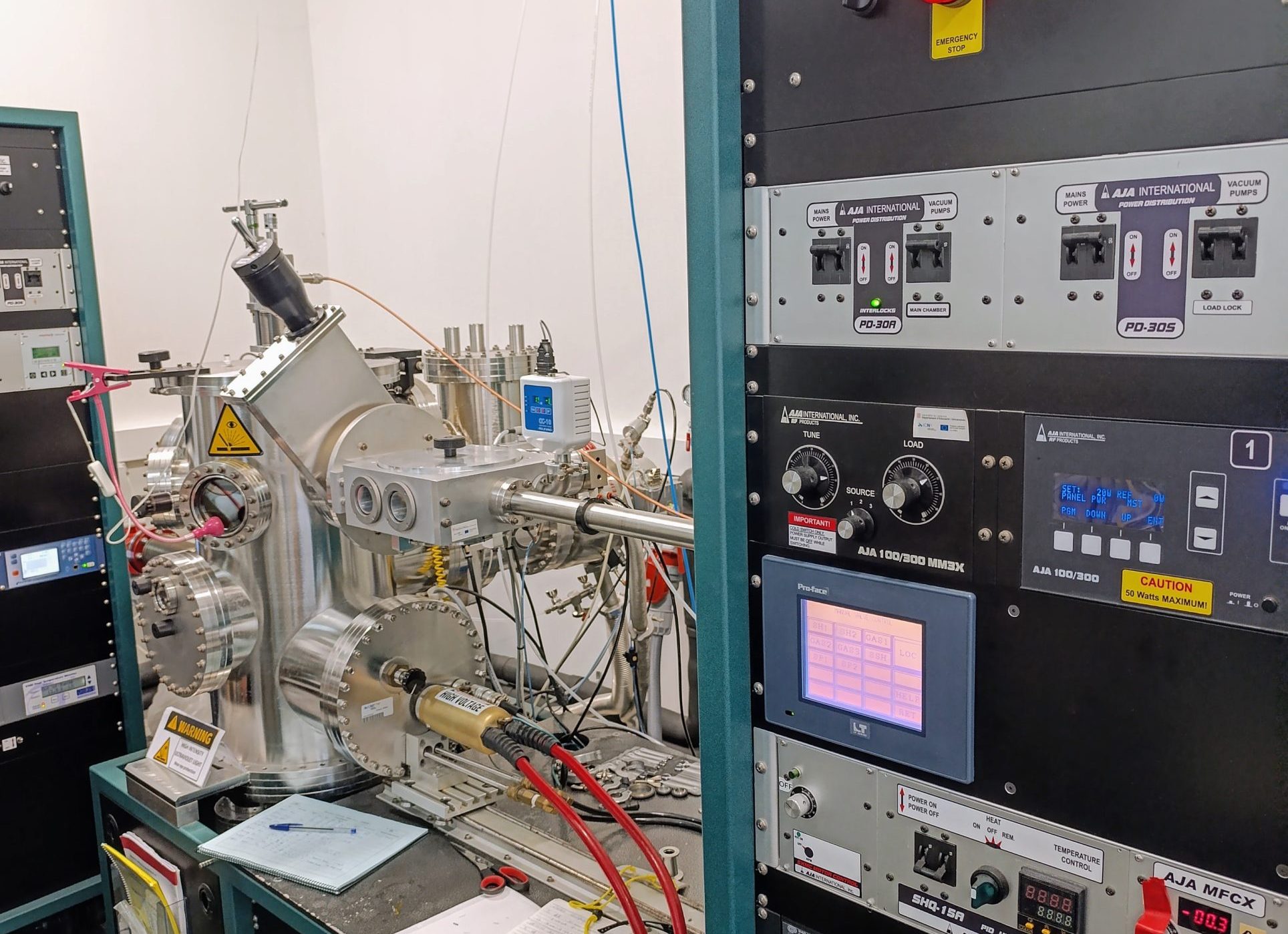
Molecular Beam Epitaxy
With our MBE we are growing topological insulators layer by layer. Operating under ultra-high vacuum conditions with dedicated chambers for different materials, it allows the grow of thin crystalline layers of materials with atomic precision.
The time lapse movie of the installation of our Molecular Beam Epitaxy (MBE) system can still be found on YouTube (Link).
Experimental setups
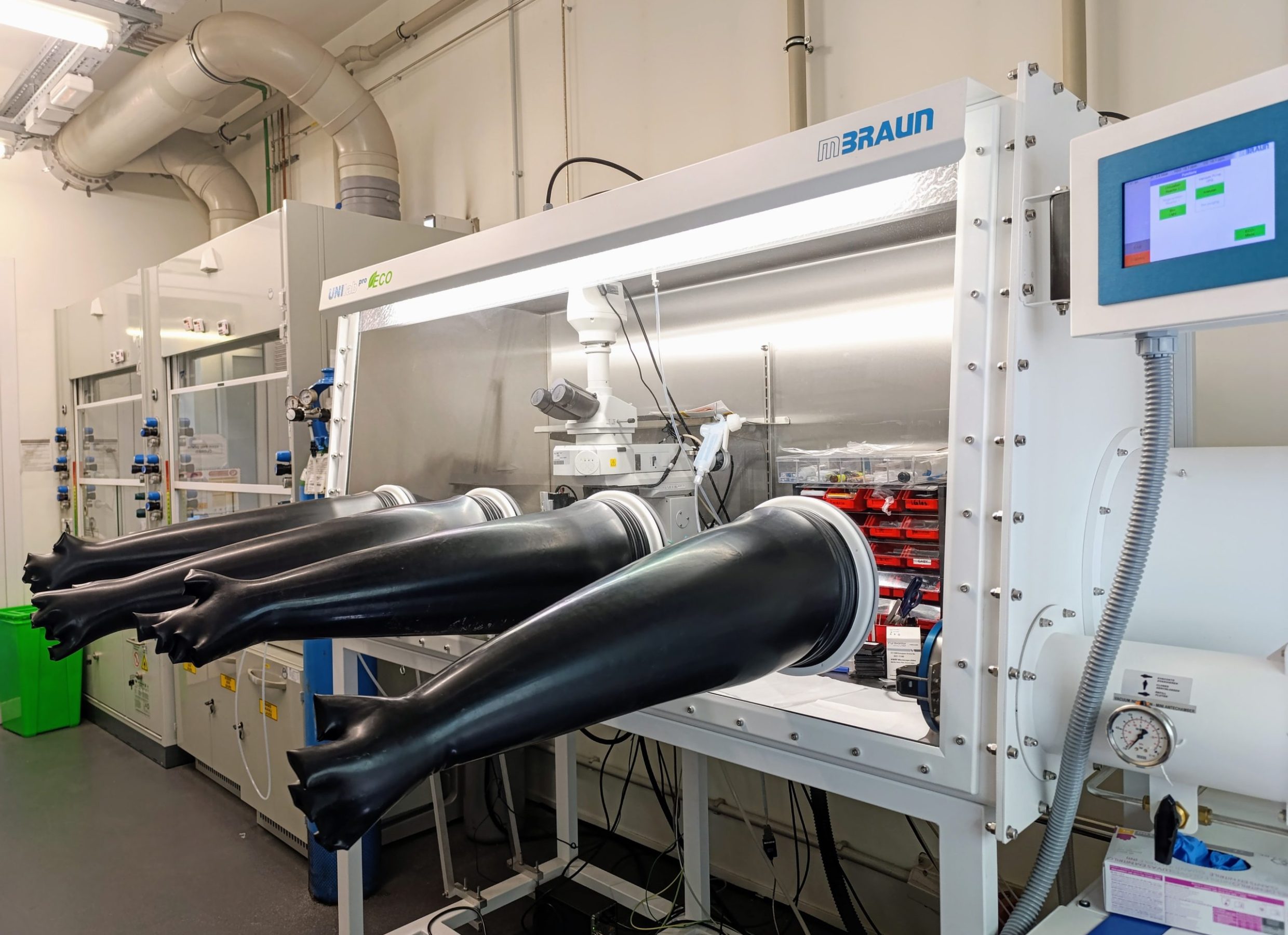
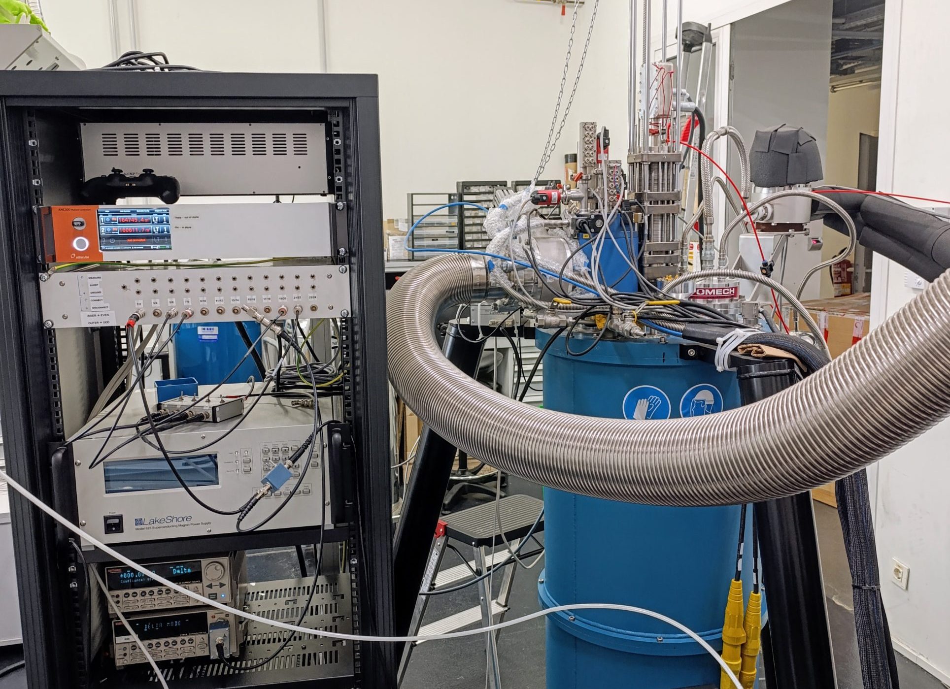
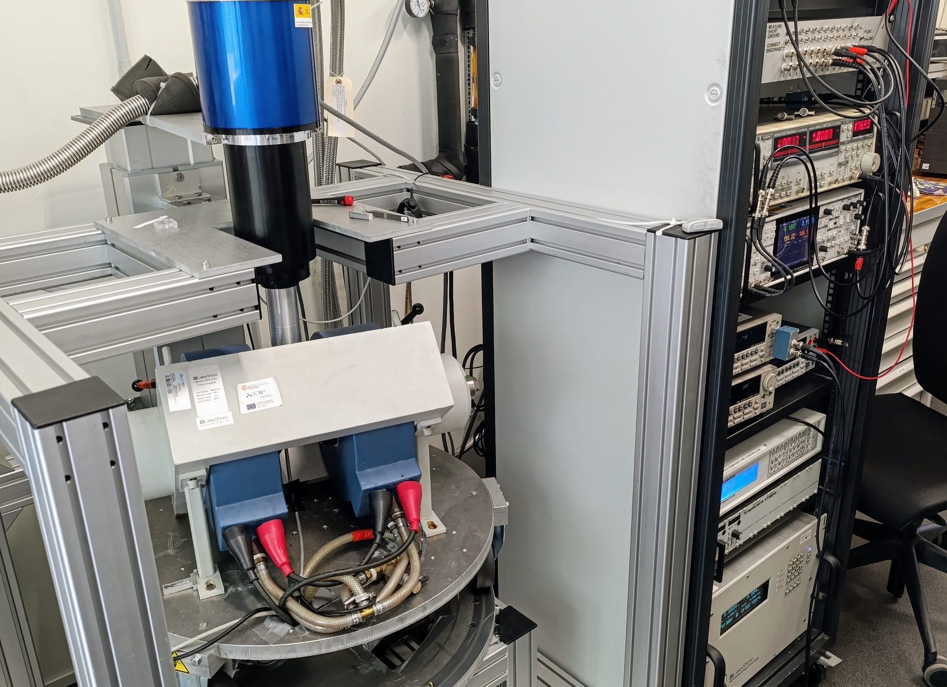
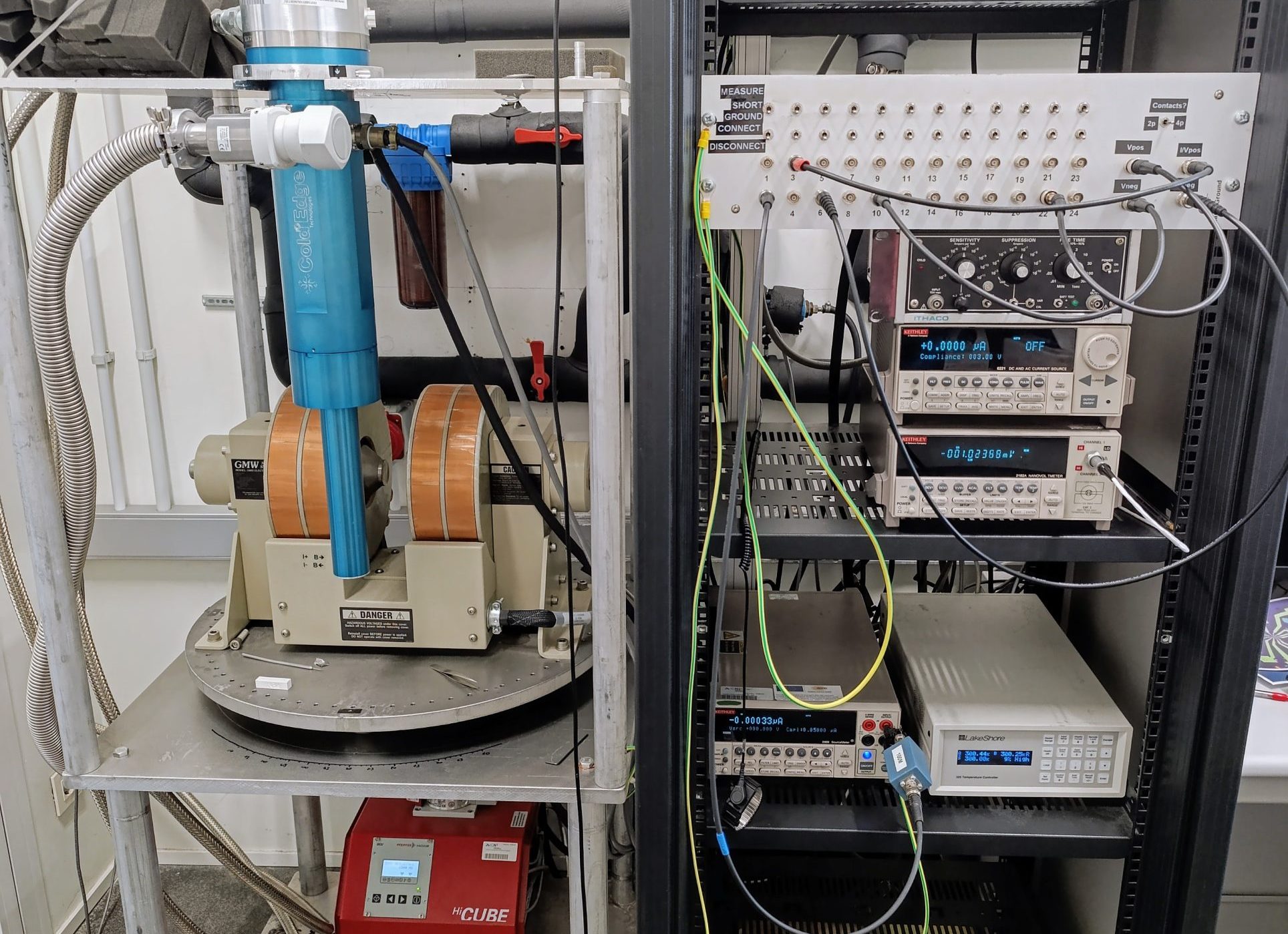
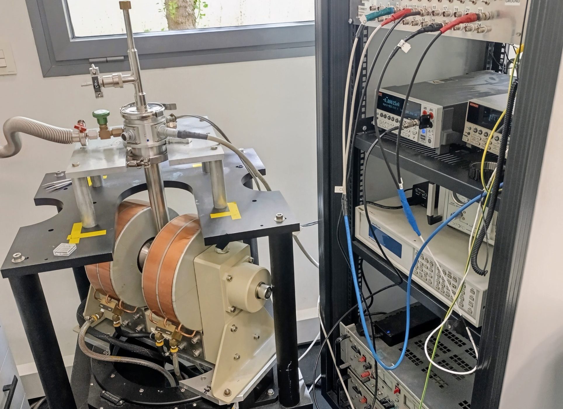
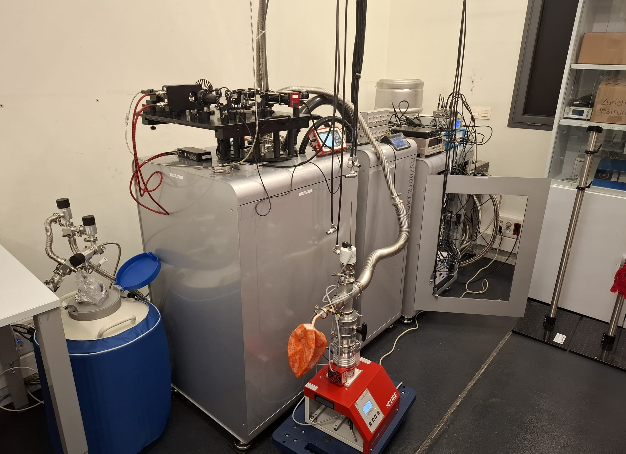
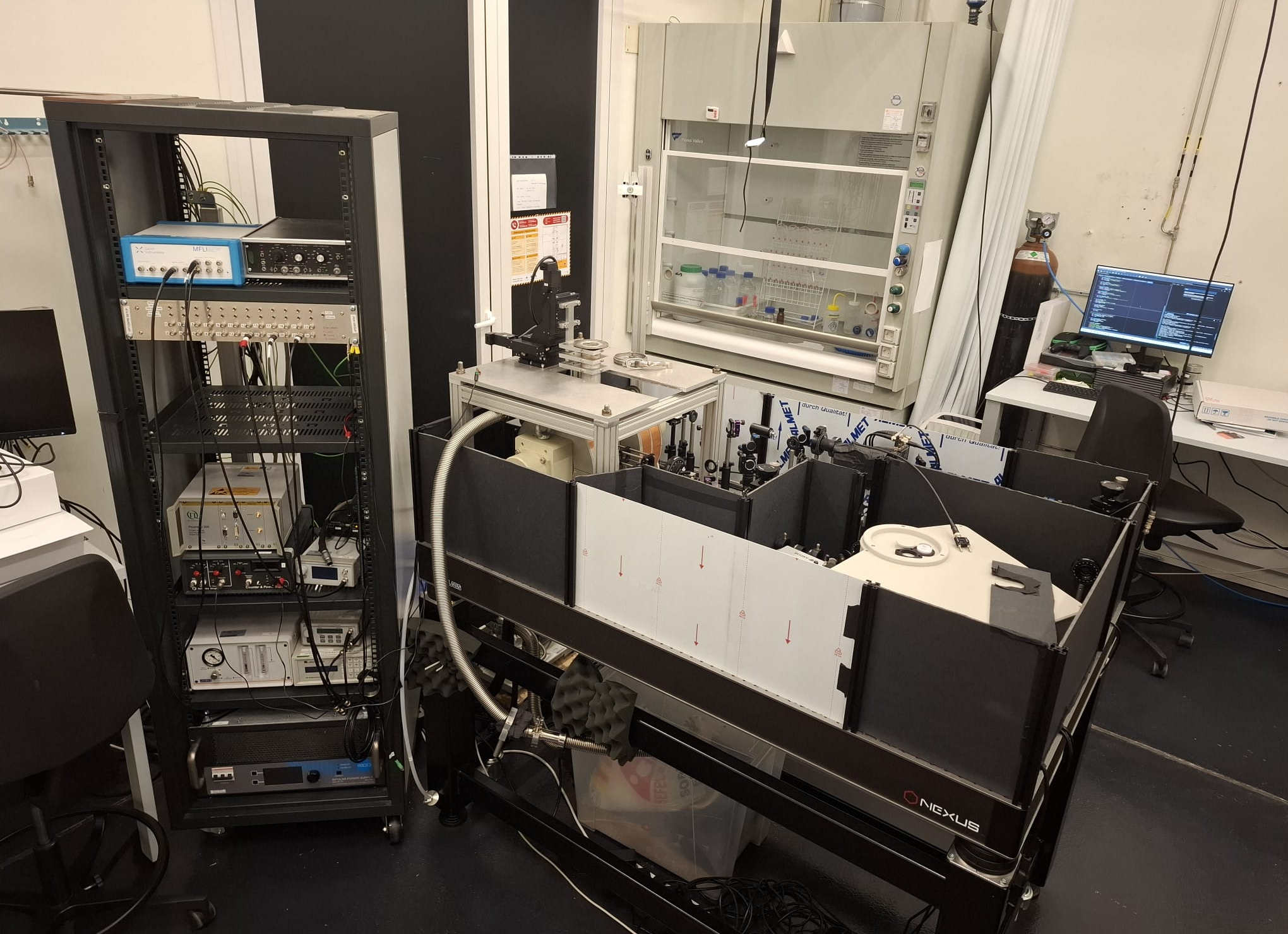
We are very well equipped for charge transport and magnetotransport experiments from low temperature (10 mK) to room temperature and with fairly large magnetic fields (9 T). We also carry out thermal and radiofrequency experiments (up to 50 GHz), as well as opto-electronic and magneto-optical experiments (with laser excitation in the wavelength range of 400 to 900 nm). For sample growth, besides the MBE, we own a CVD reactor (for graphene growth) and an atomic layer deposition (ALD) system. Inside of a glovebox, we have an optical microscope equipped with long working distance objectives and a remote-controlled three-axis micromanipulator dedicated to the transfer of 2D materials and the creation of heterostructures with them.
We are frequent (self-service) users of common facilities inside of ICN2: X-ray and angle-resolved photoemission spectroscopy (XPS/ARPES), x-ray diffraction (XRD), transmission and scanning electron microscopy (SEM/TEM), electron-beam lithography (EBL) and other cleanroom equipment. We also have strong connections to the ALBA Synchrotron next door and other institutions on the UAB campus.
Below, you can find a gallery with pictures of some of the equipment in our group.
Group pictures
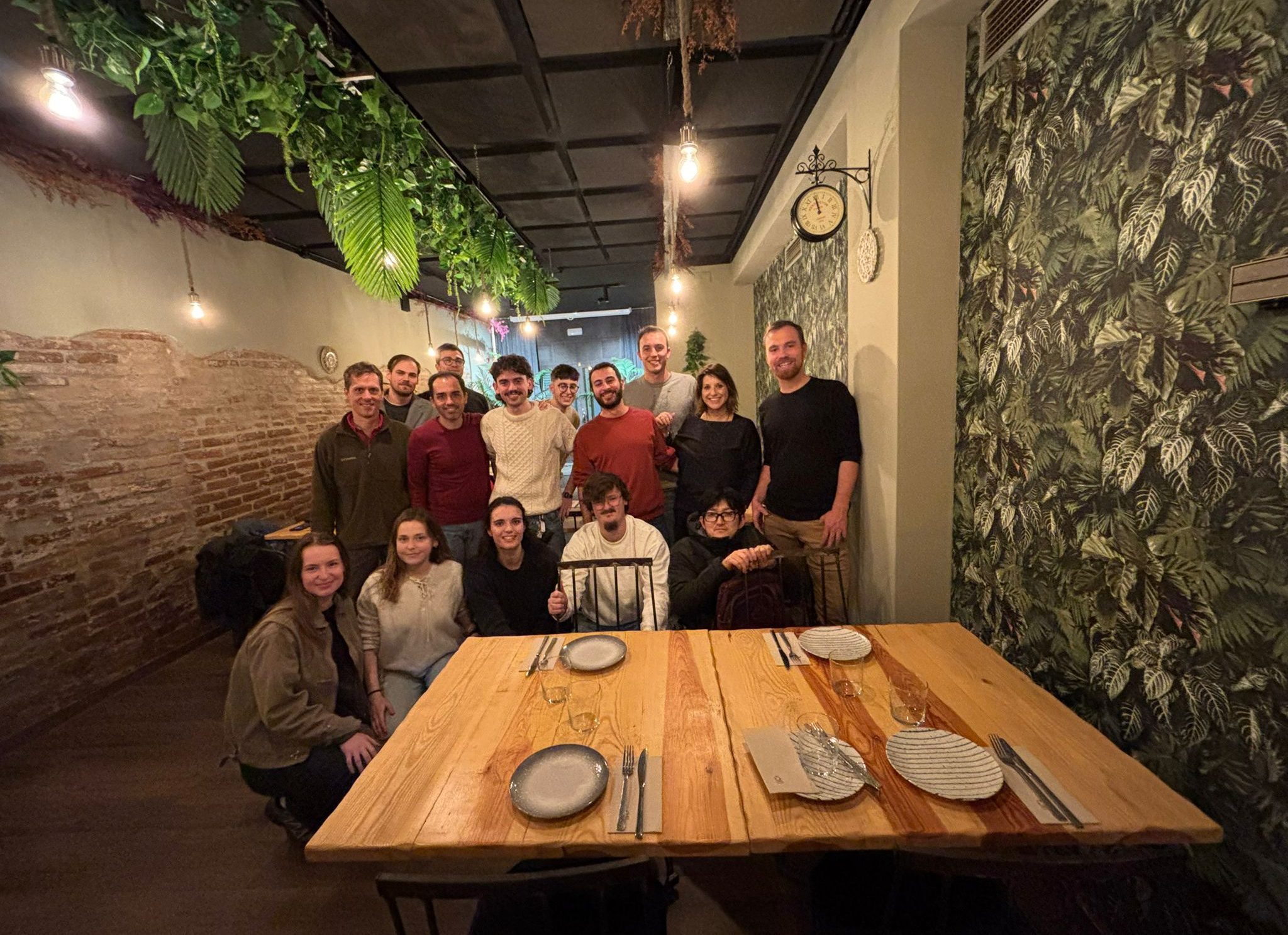
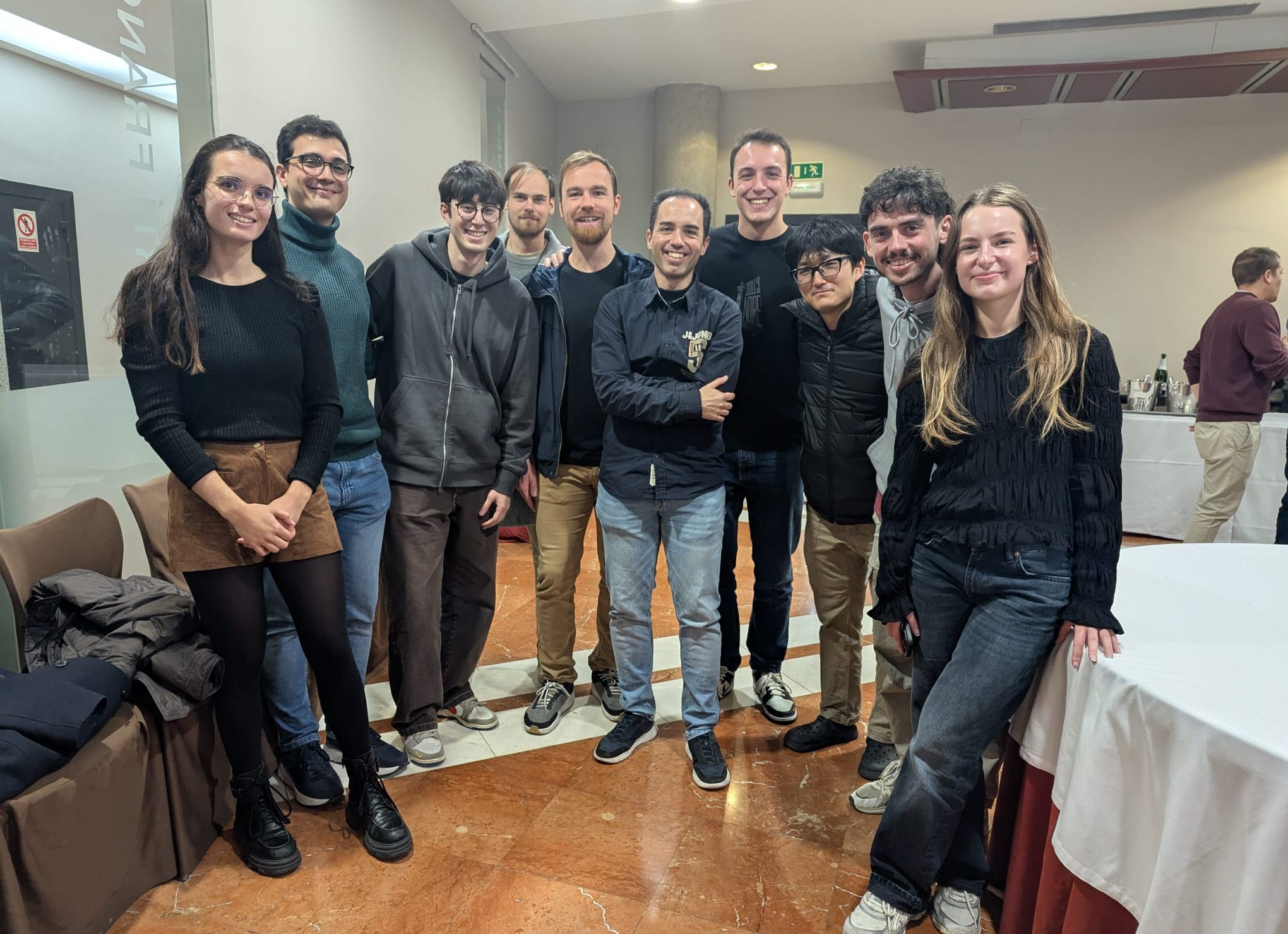
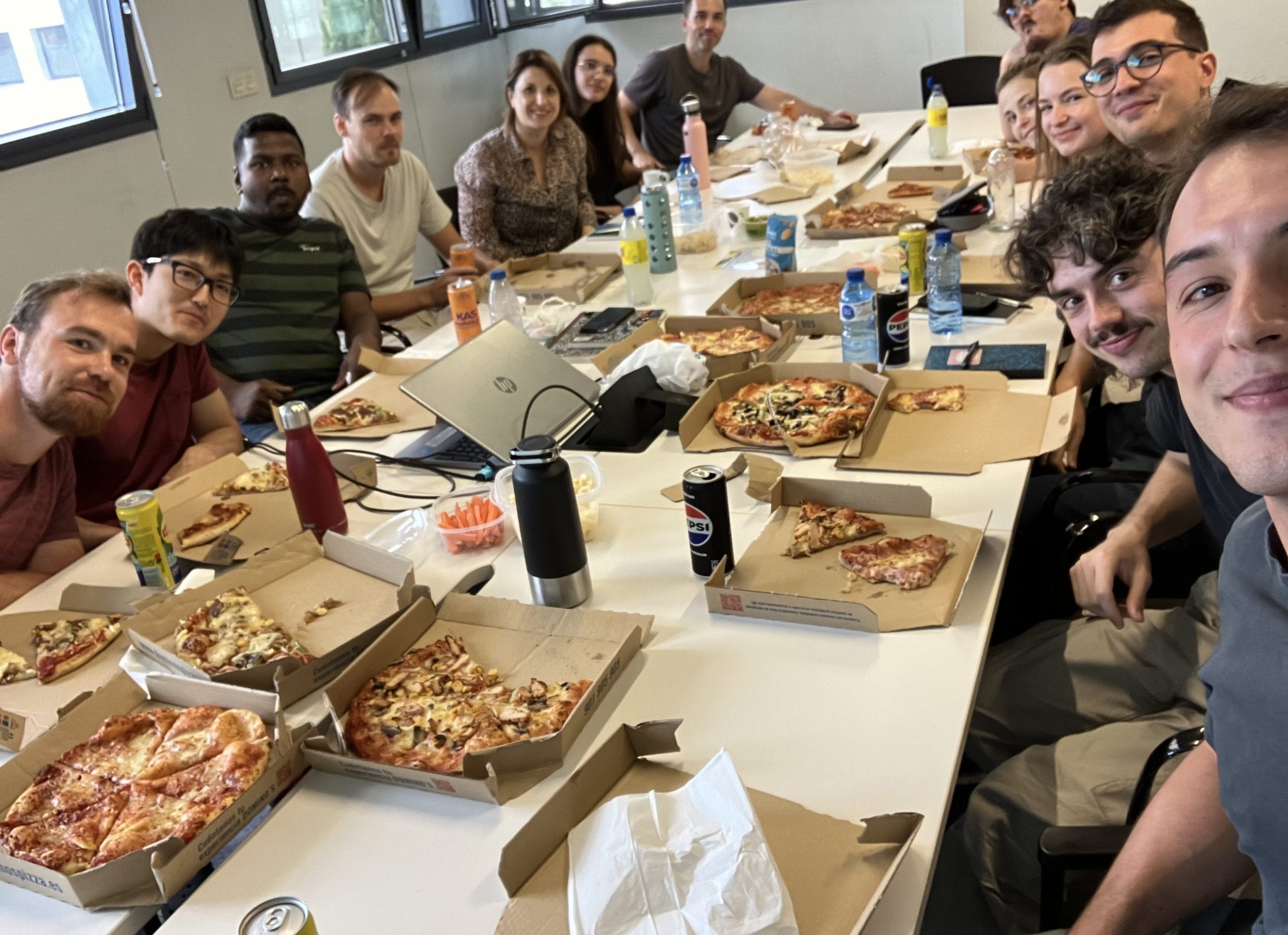
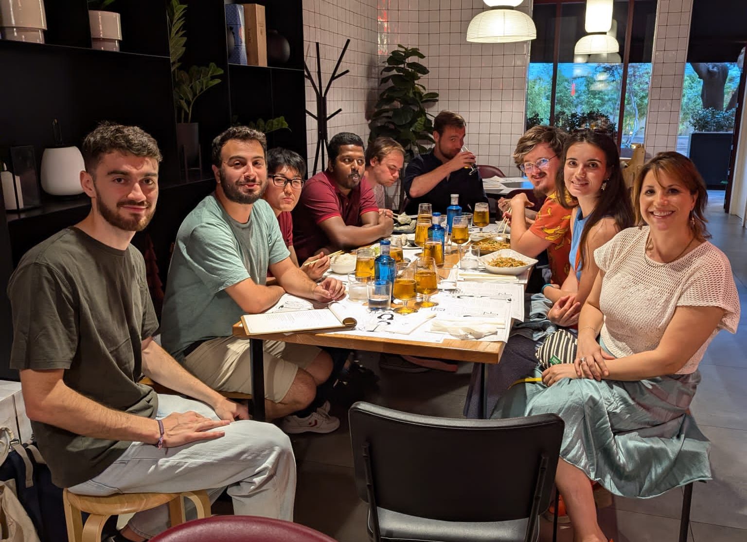
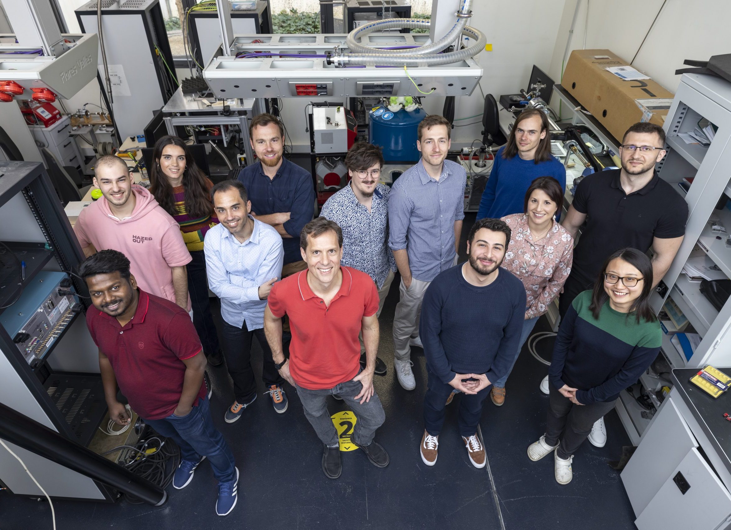
We also have a small collection of some of the group pictures, social events, workshops and conferences over the year.

